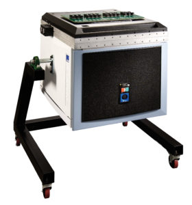
Magnum V

Magnum V

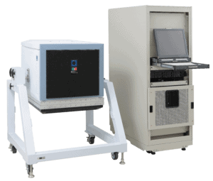
Ultra-High Performance FLASH and DRAM Memories Test Solution

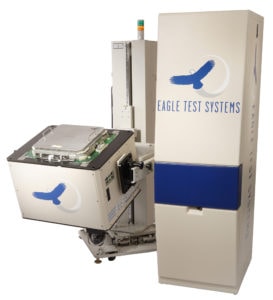
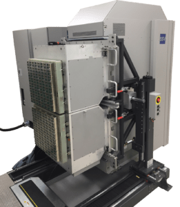
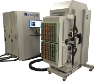
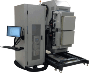
Teradyne’s Magnum V systems delivers high throughput and high parallel test efficiency for ultra-high performance FLASH and DRAM memories. Magnum V’s largest configuration delivers up to 20,480 digital channels at 1600Mbps per channel.

NAND testing

Advantages

High Performance
The Magnum V’s 1.6Gbps SuperMux mode covers today and tomorrow’s next generation ultra-high speed memory devices.

High Parallelism
The Magnum V GV can be configured for up to 20,480 digital pins to maximize the parallel test capacity for production test. The maximum number of tester resources is routed into the smallest possible area at the highest pin performance.

Scalable Platform
For each configuration, it is easy to add additional tester channels to existing “cable ready” TIU’s while maintaining DSA compatibility at the maximum parallelism for current and future devices.

Independent Site Resources
The local 3.4GHz Quad-Core site processor supports multiple test programs for concurrent test, single insertion MCP LPDDR and NAND at optional parallel efficiency.

LPDDR Feature Set
The Magnum V features pattern and timing extensions for DRAM to provide for fusion memory coverage and flash and DRAM test on a common platform.

Applications

  • eMMC
  • Toggle NAND
  • Legacy NAND
  • ONFI FLASH
  • MCP
  • eMCP
  • LPDDR2
  • LPDDR3

Configurations

Magnum V EV

  • Self- contained, low-power engineering test system for test program development and debug
  • Configurable up to 1,024 digital pins in 512 pin increments
  • Fully compatible with DSA-TCALDX and DSA on other SSV and GV production systems

Magnum V SSV (FT)

  • For final test applications
  • Configurable up to 10,240 digital pins
  • Integrated with Teradyne Vertical Plane Manipulator for efficient docking to industry standard device handlers

Magnum V GV FT

  • For final test applications
  • Configurable up to 20,480 digital pins
  • Integrated with Teradyne Vertical Plane Manipulator for efficient docking to industry standard device handlers

Magnum V SSV WS

  • For Wafer Sort applications
  • Configurable up to 10,240 digital pins
  • Uses Teradyne standard 520mm probe card standard wafer sort interface
  • Designed to adapt to third party column manipulator that minimizes the ceiling height specifications

System Options

Final Test “Tester Interface Units” (TIU’s)
The SSV and GV TIU’s interface 1.6Gbps digital channels to the handler DUT contactors. Handler specific TIU’s are available for multiple Techwing and Secron device handlers including TW322, TW-S7, TW350, and STH5600. Magnum V TIU/DSA interface technology provides maximum signal performance with a single cable direct interconnect to the DSA (socket board). This eliminates the need for costly 3rd party motherboard/cable/socket board tooling.

Wafer Sort TIU’s
The SSV wafer sort TIU employs the K52 probe interface used on multiple Teradyne wafer sort system configurations. The wafer sort SSV TIU can be swapped with any final test SSV TIU to provide for maximum flexibility in the production test environment. Magnum V K52 interface provides a direct dock, tower-less connection to the probe card for lowest cost and maximum performance.

DSA Style TCALDX Calibration
The DSA TCALDX options are handler specific calibration units specifically designed for a customer selected TIU. Once a Magnum V is calibrated, the calibration tables match the customer device specific DSA’s that are loaded into the TIU.

Interface Solutions
DSA Style TCALDX, DUT BD Stiffener Kits, Probe Card Stiffener Kits, Contactors

Software

Magnum operating system is a DUT-based multisite architecture. Magnum’s software has been architected to provide test engineers with true device-oriented parallel test programming environment. A test engineer writes a test program for a single device and the systems hardware clones the tests into multiple sites automatically. Test programs developed on the Magnum V EV can be used on production version Magnum V’s to maximize parallel test. All the software tools are site savvy, enabling test engineers to investigate device performance, on any DUT site, as though it was a one-site tester.

Ground Maintenance

Products for ATE Applications

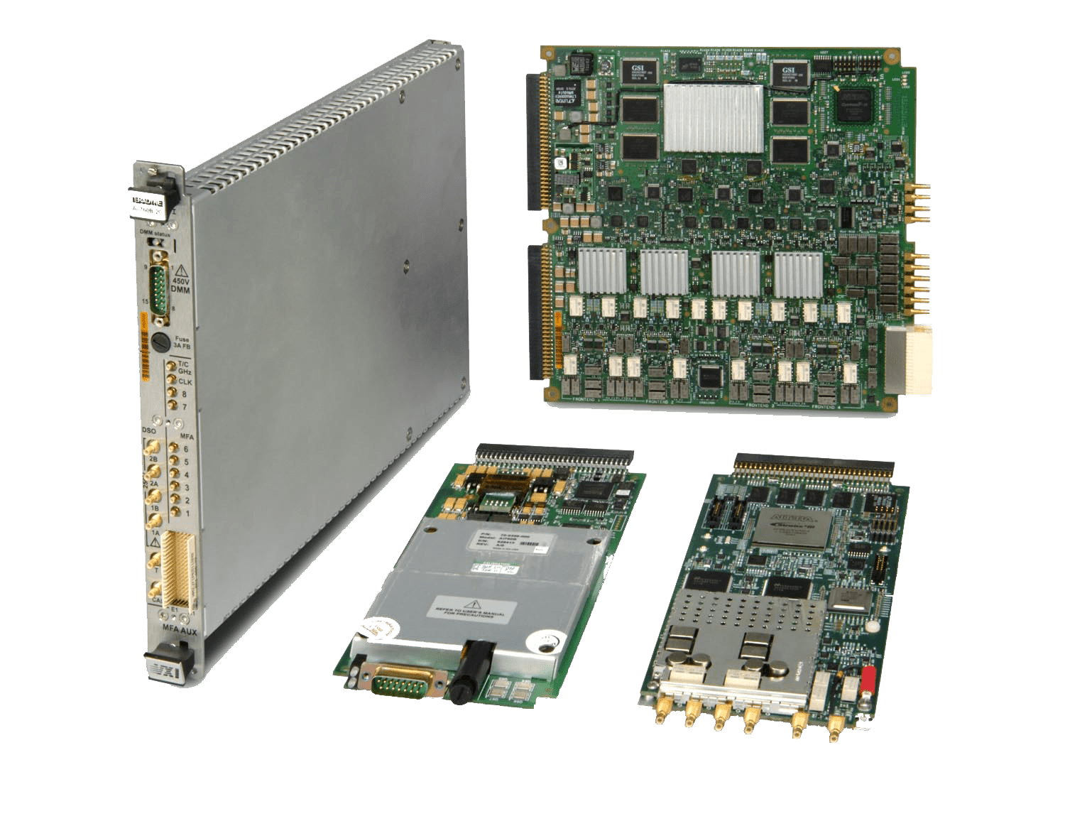
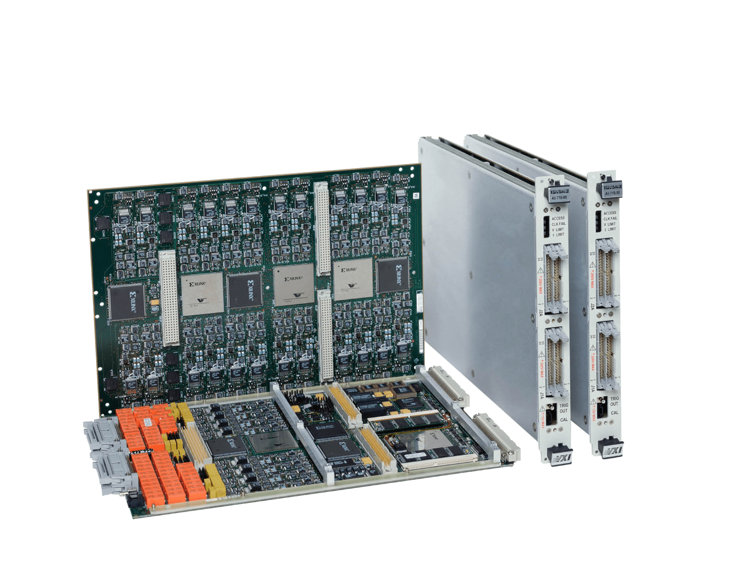
AIT provides comprehensive support for both the latest and legacy avionics interface technologies with test instruments supporting

AIT’s instruments come in a wide range of form factors including instruments for legacy ATE platforms like VME and VXI, and also instruments for the very latest ATE platforms such as PXI Express.

AIT’s avionics bus and network interface instruments are also supported by a comprehensive suite of software tools and are backed up by AIT’s expertise. From test instruments and drivers to complete PXI Express based Hardware-in-the-loop test & simulation systems, AIT provides a wide range of products and solutions supporting avionics system integration and test applications.

AIT provides software data loaders and avionics bus and network analysis tools for use in aircraft maintenance operations.

AIT also provides rugged flight ready appliances for flight test applications. With expertise in high speed network technologies such as 10G Ethernet and Fibre Channel, AIT provides cutting edge data acquisition solutions for flight test applications on the latest avionics systems and technologies.

Defense & Aerospace Home Page

Titan

Titan Asynchronous System Level Test Platform

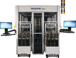
The Teradyne Titan™ System Level Test (SLT) platform delivers maximum flexibility, scalability and density in semiconductor test environments that require the highest levels of system performance testing. Titan is Teradyne’s solution for high-volume mobile application processor SLT requirements.

Semiconductor components continue to grow in complexity as process nodes shrink. IC designers are now designing complete System-on-Chip (SoC) products that contain core processors, analog I/O, digital I/O, modem and/or other IP blocks along with embedded software. Utilizing System Level Test as a third test process step, following wafer and package test, enables the semiconductor manufacturer to test software and hardware together to validate connections between IP blocks in a manner that isn’t otherwise practical. Titan provides the additional test coverage needed to meet stringent end customer failure rate requirements for improved product quality.

Production Proven Solution

Titan’s asynchronous slot architecture offers unmatched operational efficiency. It optimizes utilization and provides a 30% throughput advantage over traditional batch systems, thereby lowering the cost of test across a large mix of products.

The asynchronous slot architecture also provides the unique ability to test two different products at the same time on the system, while the internal robotics vision system ensures high placement accuracy of the semiconductor device into the test fixture. The test fixture integrates into the system with a high signal integrity interface using ATE style interconnects, providing up to 20Gbps data rates with reliability exceeding over 100k test insertions.

The asynchronous testing capability also enables maintenance to be performed without stopping system operation.

The modularity of the Titan system provides production proven flexibility to test various device package types including PoP, BGA, PGA and LGA. Its flexibility enables customers to integrate existing hardware into the functional rack, slot and/or carrier. This reuse of hardware and software allows for test program commonality, faster deployment of programs and efficient program support.

When product change-over is required, an automated process minimizes the time needed to execute changing the product to be tested.

Titan is offered as either a 320 or 424-site system with the same small footprint, enabling a high number of devices to be tested per square meter of factory floor space.

A smaller 20-site Titan development station is also available for DUT board design verification testing, developing and validating test programs, troubleshooting DUT board HW issues, DUT board test and repair activities, and enabling SLT in non-production environments.  This development station allows R&D, QA and Production to use the same DUT test board, enabling a faster ramp to production with a common engineering and production platform.

Want to learn more? Download the System Level Test white paper.

Baseline Configuration

System Mainframe

  • Up to 424 test sites per system
  • Slots are fully asynchronous for both loading and testing
  • 15°C air cooling for up to 50W of heat dissipation
  • Up to 15 fail bins available
  • Test sites can be serviced while the system continues operating

Asynchronous Test Slots

  • 1Gbps Ethernet port per test computer
  • 1 Serial port per DUT
  • 1 JTAG enabled port to each DUT
  • 1 SPI interface to each Test Board
  • VTESTBOARD Power Supply: 24V
  • Sustained DUT + Test Board Power: 38W max per site
  • Power control/measurement

Change Over Kit

  • Titan’s architecture enables device transition flexibility with low changeover time and reduced cost
  • Minimal Teradyne or customer-developed components are required for each device type change:
    • Socket lids (Teradyne)
    • DUT shuttles (Teradyne)
    • Updated device specific vision job (Teradyne)
    • Test board and socket (Customer or Teradyne)

Magnum 2

Magnum 2

High Performance, Low Cost, High Efficiency, Parallel Memory Test Solution

Teradyne’s Magnum 2 test system delivers high throughput and high parallel test efficiency for high performance non-volatile memories, static RAM memories and logic devices.

Advantages

Scalable Platform

Scales from low-channel count engineering solution to high-channel count production solution with superior throughput and high parallel test efficiency

Highly Parallel NOR/NAND Flash Device Test

  • Tests up to 80 NAND Flash devices with up to 16 device signal pins
  • Tests up to 20 NOR Flash devices with up to 64 device signal pins
  • Tests up to 160 serial Flash devices with up to 8 device signal pins

Dual Bank ECR

  • Includes hardware acceleration and RA processor
  • Simultaneous capture and scan reduces test time

Full Speed ECR

  • 800Mbps capture on all channels

Unique Data Behind Each Channel

DRAM eFuse and NAND Bad Block management per DUT

Logic Test Coverage

  • Mixed Patterns
  • Full APG with Topo Scrambling
  • Full Logic pattern sequencer with LVM vector memory per pin
  • APG + LVM sequences in the same pattern

Applications

Memory

  • NOR Flash
  • NAND Flash
  • SRAM
  • DRAM
  • MEMs

SOC

  • Microcontroller
  • Low-end SOC
  • Converters

Configurations

Magnum 2 EV

  • Self- contained, low-power engineering test system
  • For customer and Lab applications that require test program development and debug
  • Up to 128 digital I/O pins plus an option board (DPS, VRC, or MPAC)
  • Internal air compressor eliminates need for facility compressed air to operate the load board latch mechanics
  • Runs on standard 110 VAC power (220 VAC Europe)

Magnum 2 PV

  • Five-slot chassis supports up to 640 digital I/O pins in 128 pin increments
  • Can be configured with multiple DPS, VRC, or MPAC option boards matched with the appropriate number of digital I/O channels to meet the requirements for complex memory and logic applications

Magnum 2 SV

  • High-mix production solution
  • Up to 1,024 digital pins for parallel test
  • Final test and wafer sort production
  • Compatible with industry standard handlers and wafer prober, including hinge and column  manipulators

System Options

MPAC

  • Analog source and capture option
  • Available with 24- or 48-channels of source/capture/Vref
  • Voltage reference for multiple test applications including embedded converters
  • Integrated parametric measurement unit (PMU) available at any instrument channel


DPS

  • Option for testing low pin count devices that must be tested highly parallel
  • Maximize resource utilization and device parallelism
  • Available in 32- and 64-channel configurations


MPAC24/DPS32

  • Option is a combination of 24 MPAC channels and 32 DPS channels


TCALDX

  • High-throughput, low-cost digital channel calibration option
  • Hardware and software solution calibrates system faster than the “relay-tree” calibration technique


Traceability

  • NIST certified instruments to support traceability (Magnum 2 systems do not directly support NIST compliance)
  • For AC measurements, TCALDX port provides access to the internal crystal of Magnum 2’s AC sub-system, one per site assembly. The timing path is routed through a digital counter cable to a NIST Certified Stanford Research SR620 counter (or equivalent) to provide a path for AC traceability
  • For DC measurements, TCALDX port provides access to a reference voltage from Magnum 2’s DC sub-system. Reference voltage is sourced from each DP board on a site assembly and routed through a digital multimeter cable to a NIST certified Agilent 3458A multimeter (or equivalent) to provide a path for DC traceability


Interface Solutions
DIB’s, PIB’s, Loadboards, Calibration BD’s, DUT BD Stiffener Kits, Probe Card Stiffener Kits. Final Test Interfaces, Wafer Probe Interfaces, Docking Solutions, and Test Cell Integration

Software

MagnumUI Software is a DUT-Based Multi-Site Architecture that has been architected to provide test engineers with true device-oriented parallel test programming environment. A test engineer writes a test program for a single device and the systems hardware clones the tests into multiple sites automatically. Test programs developed on the Magnum 2 EV or Magnum 2 PV can be used on the production version of Magnum 2 to maximize parallel test. All the software tools are site savvy, enabling test engineers to investigate device performance, on any DUT site, as though it was a one-site tester.

IP750Ex-HD Family

Image Sensor Test System IP750Ex-HD

The Global Leader in Image Sensor Testing

Why does the IP750Ex-HD lead the market? It’s a trusted fourth-generation test system that delivers image sensor test capability for current and future devices while providing the lowest cost of test.

IP750Ex Image Sensor Test System

Our customers know that Teradyne’s worldwide applications support provides unparalleled test expertise. All of which may explain why the image sensor market has consistently selected the IP750Ex-HD Image Sensor Test System as their test solution.

The IP750EX-HD has been the test platform that has enabled the industry to manufacture high quality CCD and CMOS image sensors, and it is the most economical platform to meet the needs of newer technologies such as Time of Flight (ToF) sensors. When you use a smartphone, high performance digital still camera, or in-home security and surveillance system, these applications have image sensors most likely tested by Teradyne’s IP750ExHD.

As image sensors are being designed with more features, Teradyne’s IP750Ex-HD continues to expand test coverage. “Sensing” devices now include distance ranging, 3D depth sensing, Augmented Reality (AR), Virtual Reality (VR), automotive safety and Advanced Driver-Assistance Systems (ADAS) applications. Mobile applications are increasing the adoption of multiple cameras and fingerprint scanning camera for user authentication. The increased complexity of the device design increases test time. And, automotive applications are seeing increased test insertions impacted by low and high temperature test at the packaged device test.

How do we improve test times and time to market as image sensors become more complex? Teradyne’s IP750Ex-HD operates with the award-winning IG-XL™ software. Image Sensor vendors know that the user-friendly software provides the fastest time from R&D to production.

The IP750Ex-HD is architected to meet the increasing demands of higher resolution image sensors, expanding test quality standards, and innovative new sensor features with varying wavelengths of light and modulation features.  The architecture supports 64-bit image data processing to meet the processing demands of increasingly higher resolution sensors, and the data transfer utilizes the fastest data busses to ensure that the fastest test times are achieved.  While Teradyne provides image processing libraries and applications expertise to make it easy for test engineers, IG-XL™ also allows customers to implement customized image test algorithms to both create and protect their test IP.

Advantages

Powerful bank of processors for running the most advanced image test algorithms for high resolution devices

High speed parallel data transfer at 40Gbps per instrument

Up to 80 sites in parallel test

Scalable computing and high data movement architecture ensure the lowest cost of test across all sensor types – from low site count specialty sensors to high volume image sensors

Secure and easy support for customer proprietary test algorithms

Broad Device Coverage

  • High versatility for testing a broad range of devices – VGA to over 100M pixels with numerous image output capture standards capability
  • Only instrument solution in the market with custom LVDS protocol coverage
  • Strong SoC test capability with digital instrument for SoC type image sensor

Configurations

IP750Ex-HD

  • 80-site system capable for wafer test
  • ICMD 1.5Gbps MIPI D-Phy image capture instrument
  • Custom LVDS capture capability with ICMD
  • D-PHY 2.5Gbps image capture unit
  • C-PHY 2.5Gsps image capture unit
  • M-PHY 6.0Gbps image capture unit
  • HSD800 400MHz Digital instrument
  • HDDPS 24/48Ch DC source
  • 40Gbps image data transfer
  • 150mm x 160mm illuminator support
  • Compatible with J750Ex-HD instruments

System Options

VI Resources

  • APMU: 64Ch, -35V to 35V, 50mA@35V capability, merge x8 /400mA
  • HDVIS: -10V to 10V, 200mA@10V capability, merge x4/800mA

Converter Test

  • CTO: 8 Source, 8 Capture, 16-bit ADC testing
  • HDCTO:  32 Source, 32 Voltage Reference, 8 Capture, 14-bit ADC testing

ETS-88

ETS-88

Test System Optimized for High Throughput, Low Cost of Test for Single Site, Multi-site and Index Parallel Applications

eagle test systems ETS-88

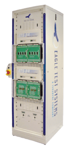
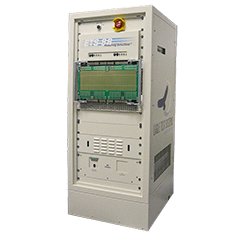
The ETS-88 is an optimal test platform for testing a wide variety of devices including: simple analog, high precision, high voltage, high current / power, automotive, video, audio, complex mixed-signal, as well as emerging power processes like SiC and GaN. The ETS-88 test system hardware is designed to provide independent floating resources per site to avoid resource sharing across sites while improving site-to-site isolation and measurement accuracy.

Advantages

Multi Test Head design supports high parallel test efficiency, capable of testing up to four unique DUTs per test system in 1 square meter of floor space. Each test head offers up to 72 analog channels and up to 32 digital channels (66/132 MHz).

Industry leading EV software operating from a dual quad core CPU controller supporting both index parallel and multi-site test.

Fully compatible with ETS’s line of Digital and Floating SmartPin™ Resources.

Test system PC runs on familiar MS WindowsTM operating system and executes programs from C++ Visual StudioTM environment.

Applications

Power Management

  • Low dropout regulators, DC-DC converters, voltage regulators, boost regulators, multi-phase PWMs, battery chargers, hot swap power managers, gate drivers

Precision Analog

  • Op amps, instrument amplifiers, video amplifiers, audio amplifiers
    automotive
  • Fuel injectors, ABS controllers, airbag controllers, automotive smart switches, CAN transceivers, motor drivers

Discrete & Power Modules

  • MOSFET, IGBT, diodes, BJTs
  • Consumer SPM/IPM, industrial solar/UPS/motors, automotive HEV/IEV/SSV

Converters and Mixed-Signal

  • Low-speed/high resolution D/A converters, high-speed D/A converters, low speed/high resolution A/D converters, high-speed A/D converters, CODECs

Configurations

The ETS-88 multiple test head architecture provides the flexibility to reconfigure the test system using software control. The system is comprised of dual sector test head card cages for up to four sectors depending upon system configuration. Each set of sectors can be bridged together within the test head card cage on an application-by-application basis. The sectors can be configured to operate independently, running unrelated applications if desired, or can all be bridged together to expand the site count of multi-site applications.

The system is controlled using a multi-core PC to maintain isolation between applications. This control method lets you assign cores and test heads to applications for the greatest test efficiency, and provides the ability to support single site, multi-site, and I.P. applications from a common base platform.

eagle test systems ETS-88

ETS-88 Standard Configuration (Up to four sectors)

  • Up to 32 digital channels
  • Six floating resource slots for up to 72 analog channels
  • 32 C-Bits
  • Eight programmable master clock channels

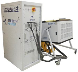
ETS-88TH/AC-2500 Configuration (two sectors)

  • 12 Floating resource slots (six per sector)
  • One DPU-16 instrument per sector (32 pins total)
  • Two HPU instruments per sector (400 A total)
  • AC-2500 card cage
    • AC instruments
    • Matrices
  • Electronic motor DIB actuator

Instrument Options

The ETS-88 test system is a general purpose precision analog and mixed-signal test platform designed for high volume production testing of integrated circuits. The system is optimized for high throughput applications, with a fully integrated multisite software and hardware architecture. The ETS-88 test system offers high precision and high accuracy test capabilities. Test speed is only of value if the results are trustworthy. As such, the ETS-88 test system provides both measurement speed and high accuracy, following the ETS tester tradition of providing high precision test capabilities with a robust assortment of available instruments such as V/Is, DC/AC voltmeters, digitizers, AWGs, digital pin electronics, and time measurement instruments, all optimized for multisite testing.

8×8 MATRIX: High voltage force / sense crosspoint matrix; any input channel can be connected to any output channel

APU-12: 12 channel, four quadrant V/I with six current ranges ranging from 200 mA to 10 uA at +/-30 V

CAMII: Instrument module designed to measure capacitance in the sub-picofarad range

DPU-16: 16 digital I/O channels supporting vector rates up to 132 MHz with 8M of standard vector memory

HCU-2000: One channel, 2000A rack mounted resource for ETS-88DUO Testhead with innovative interposer connection for fast and reliable high mechanical endurance connection and disconnection to the DUT Board.

HPU-100: Single channel V/I with 10 current ranges operating up to +/-100 V

MPU-120: Four quadrants V/I with built in 16-bit digitizer capable of forcing voltage up to 120 V and current force up to 40 Amps

QHSU: Two fully independent dual channel high-speed signal analyzers capable of source or measure up to 50 MHz

QMS / QMS-T: Four precision (12-bit at 10 Msps or 16-bit at 200 ksps) independent floating differential volt meters that support AC and DC measurements up to +/-200 V

QPLU: Low noise, analog source and measure resource with 1 PPM (20 bit) accuracy with 381nV resolution

QTMU: 8 independent time measurement units multiplexed to digital pins with a start/stop and arm signal per sequencer

SPECII: Test head expansion, relocating high power instruments to the mainframe cabinet

SPU Family (100, 112, 500): A suite of V/I’s capable of addressing a wide range of test requirements ranging from 100V / 2A to 500V / 50mA with fully AWG and digitizing capabilities per channel

WCU-2220: Waveform capture instrument with full scale sensitivity from 0.2V to 2000V at 8-bit resolution with a decade of programmable offset available per range

Software

The ETS software development environment and tool set are truly one of the strongest attributes of the ETS-88 test system. The software tools are easy to learn and use, and are fully integrated into the Microsoft Visual Studio development environment. The complete test system command set is supported with automatic code generation tools (ACE™ and GrACE™). This means that users are not required to memorize command arguments and syntax. Graphical plotting tools are provided for simple point-and-click plotting of test-oriented waveforms. RAIDE™ (Rapid Access Interactive Debug Environment) makes it easy to view and change tester hardware settings.

ETS’s software provides a robust test development environment, offering customers an easy learning curve and uncommon productivity. There are two versions of the software: EV and EV-MST. Referring to multi-sector technology, EV-MST allows users to replicate test programs across multiple test head sectors. The standard ETS-88 test system supports both software suites. Adding options, such as the AC-2500, may change which suite is supported.

EV & EV-MST Graphical Test Programming Environment

EV Key Features

  • Innovative, easy to use graphical methodology for controlling test system resources
  • Fully integrated plotting tools
  • EV advanced software tools for uncommon productivity
    • Fully support multisite parallel testing
    • Complete support of pattern-based testing
    • Graphical programming methods reduce time-to-market through the introduction of simple and easy to operate tools


EV-MST Key Features

  • EV-MST software architecture supports different modes of operation
  • Simultaneous independent applications
    • Each application can itself be multisite
    • Keeps tester utilization high by continuing to run other applications during changeover
  • Traditional multisite applications with synchronized testing on multisite handlers
    • Independent communications channels allow near 100% multisite efficiency
  • Full index parallel testing that maximizes turret handler throughput
    • Specialized datalog handling combines DUT data from different sequential stations
    • 100% resource independent QA test

As the leading provider of complete Test Cell Solutions and services, we at Teradyne leverage our expertise, experience, and technology leadership to help our customers achieve the highest yield and the highest throughput in production with the fastest time to market. We partner with you in your journey from design to production to provide standard and customized test cell products and services.

J750Ex-HD Family

J750Ex-HD Family

The Industry Standard in High Efficiency, Low Cost Test

The world produces billions of semiconductors every year, and the test requirements vary significantly. The J750Ex-HD offers the lowest cost test solution for uncompromised test quality of less complex mixed signal devices.

J750ExSystem

J750Ex-HD: the MCU Test Solution

Microcontroller Units (MCUs) are used in automobiles, mobile electronics and robotics. As you go through your day, dozens of MCUs are in your electronic devices working to provide unique features and Teradyne’s J750 family most likely tested them.  With a growing installed base of over 6,000 test systems and widely available at more than 50 Outsourced Assembly and Test (OSAT) locations, Teradyne’s J750 is the industry standard for high volume test of low-cost devices.

Why does the J750ExHD dominate microcontroller test? The J750 was first introduced in 1998. Teradyne was focused then, and is today, on reducing single site test times and optimizing parallel test efficiency to lower the cost of test while maintaining compatibility across generations of the platform. The J750 family is the longest running active ATE product which has maintained compatibility throughout its entire lifetime while providing new instrumentation to offer higher performance and lower cost of test. The J750Ex-HD is the latest offering which offers the highest level of parallelism and performance on the market.

Lowest Cost of Test

Reducing the cost of test is crucial in a highly competitive semiconductor market. The J750Ex-HD family reduces the cost of test by 25-50% over competitive offerings with higher throughput and increased site count. Higher site count is delivered by the High Density (HD) family of instruments and software providing the fastest path to lowest cost of test.

Fastest Time to Profits

The award-winning IG-XL™ software enables thirty percent faster development of multisite test programs compared with competitive ATE software systems. IG-XL is focused on efficiency requiring 50% fewer lines of code compared to other ATE programming languages. The software environment encourages code reuse, and the real-time debug experience is significantly enhanced by language that does not require compiling of code. Because the software transfers seamlessly within the J750Ex-HD family, there is lower risk in production implementation by leveraging current docking interfaces for production floor integration.

The J750Ex-HD is well-known for its ‘zero footprint’ design minimizing use of valuable manufacturing floor space. The scalability of the test system, to 2048 multifunction pins and data rates up 400 MHz/800 Mbps, makes it ideal for low-cost devices with increasing feature integration.

Test Quality for Automotive MCUs

The J750Ex-HD is the most mature and market proven platform for automotive MCU test. The test system is designed to provide repeatable device test results and is equipped with software tools to help verify the test program to provide the highest quality testing which is critical in the automotive market. A test program verification tool suite prevents programming errors and unexpected program changes. Unique instrument monitoring features avoid latent damage to devices, and a tri-temperature probe interface means automotive devices can be tested at cold (-25 to -45°), ambient and hot (120 – 160°C) temperatures.

J750Ex-HD Options for Testing All the Components Inside of MCU’s Include:

  • High Speed Digital 800 instrument (HSD800) provides digital functionality and characterization test
  • Memory Test Option (MTO) for embedded memory test
  • Digital Signal Source & Capture (DSSC) behind each pin for memory and mixed signal
  • Deep Scan History RAM (DSHRAM) for DFT based SCAN test
  • High Voltage Digital (HVD) function for embedded flash testing
  • High Density Device Power Supply (HDDPS) for high performance precision-controlled device power
  • High Density VI Source (HDVIS) for high site count and pattern controlled for precise timing of test measurements
  • Mixed Signal Option (MSO) for audio testing of embedded analog components
  • High Density Converter Test Option (HDCTO) for testing embedded ADC/DAC converters
  • High Density Analog Pin Measurement Unit (HDAPMU) for mixed signal test

J750 – LitePoint RF Test System

The option of adding LitePoint instrumentation to the J750 system delivers a cost-effective, complete production test solution covering global wireless connectivity standards. With the proliferation of embedded RF components such as Bluetooth® into microcontrollers and other stand-alone wireless SoC devices, the J750 can test an even broader range of applications while continuing to deliver superior cost efficiency and fast time-to-market. By utilizing the same LitePoint instrumentation that the engineers do initial bench bring-up and downstream module testing, the total effort and time to get to market with new products is improved significantly.

Available as an upgrade for all J750 models (J750, Ex, HD), the J750-LitePoint leverages IG-XL for development and debug and incorporates the LitePoint RF Tool Suite and modulation libraries. The J750-LitePoint provides dedicated onboard-instrument DSP for high-throughput RF signal processing, an extensive wireless software library and a comprehensive debug tool suite.

The J750-LitePoint is compatible with existing LitePoint applications. The test system supports up to 32 RF ports enabling high site count with a reliable signal interface for 6GHz performance to the device interface board.

As the leading provider of complete Test Cell Solutions and services, we at Teradyne leverage our expertise, experience, and technology leadership to help our customers achieve the highest yield and the highest throughput in production with the fastest time to market. We partner with you in your journey from design to production to provide standard and customized test cell products and services.