Device Interface Solutions
Device Interface Solutions is being acquired by Technoprobe. For more information, please read the press release.
Enabling Optimized Testing of the Next Generation of Technology
Complex ICs require high-performance testing capabilities and Teradyne’s DIS are all about performance. Couple our industry-leading performance with our dependable quality and reliable on-time delivery (OTD), and the result is a successful equation for a lower total cost of ownership (TCO).
Calculate Your Savings
Use the DIS Total Cost of Ownership Calculator to evaluate with your own numbers, how much you can save by using Teradyne Device Interface Solutions.
Why are complex device manufacturers turning to Teradyne’s DIS?
DIS understands complex devices and delivers a lower cost of ownership solution for our customers. To achieve the best test economics, we prioritize performance. Performance means maximizing power and signal integrity for higher parallelism, better IC yields and faster test (scan clock rate). We deliver quality which means defect free hardware on the first day and higher up-times throughout production. DIS is committed to reliable On-time Delivery (OTD) for both New Product Introductions (NPIs) and repeat orders which allow our customers to plan productions ramps and support their end customer demand. We focus on efficient development and manufacturing to support shorter lead times and we meet the requirements, on the first attempt, to support first wafer validations and volume production ramps. Complex device manufacturers turn to DIS because we consistently deliver on each of these critical elements which allows them to achieve a lower cost of ownership.

Device Complexity
In semiconductor test, the era of complexity is here…and evolving. In fact, device complexity trends are increasing at a rate of 2x pins, 2x performance every four years. This development, known as 2×4 scaling, brings with it increased probe card complexity and the need for a system development approach in the interface hardware lifecycle. While complexity is significantly increasing the size of devices is drastically decreasing. Currently, 5nm is an industry norm for the size of a complex device. However, by 2025 designers will be working in the 2-3nm range. Will today’s test strategy be ready? Interfaces are becoming as complex as test instruments.

Interface Hardware Complexity
Complex devices have unique pin density, speed, power and thermal requirements to consider. DIS recognizes increasing Device Under Test (DUT) sites and pin count drive up the pin area density which requires routing the I/O and power to the DUT with an increasing mechanical load. Complex devices require connections to high performance I/O such as high-speed digital, wireless and high voltage which can create a signal integrity issue when combined with very tight pin and DUT spacing and high DUT count. Power requirements mean a large number of high current (>25A) device supplies require excellent precision combined with a voltage reduction (<700mV) and increasing number of power rails. Finally, we understand how critical it is to remove DUT thermal energy due to self-heating and support increased operating temperature ranges while increasing transistor counts combined with tight DUT spacing rapidly increases thermal density.
And, market windows are short for complex devices. Add to that cloud computing and storage costs drop approximately 50% every three years. Clearly, AI, RF, PMIC, high end mobile and high-performance computing applications are driving new economics that must be evaluated and optimized in many areas – leading to an understanding of total cost of ownership.

Systems Development Lifecycle
Complexity management principles require an integrated systems mindset. That means each development phase communicates with the others. Each major phase of the interface lifecycle is interdependent on the other with the quality of the feedback in each phase impacting the overall robustness of the system.
The systems development approach includes: interface design, interface manufacturing, performance verification, diagnostics/QC, maintenance and service, and production operations support. The goal of this approach is a fully integrated design and manufacturing solution. Rigorous specification and quality management avoids the costly mistake of passing along defects. Complete with integrated certification, repair, maintenance, calibration and Bin-1 validation. An integrated design and manufacturing system is able to scale effectively as complexity increases.

Total Cost of Ownership
Interface hardware complexity has an impact on time (both production test times as well as production release timing) and yield. The TCO model builds on previous models to include the effects of time and entitled yield which are key metrics across the value chain for a semiconductor company. The four main phases of a semiconductor development lifecycle, from a test perspective, include: interface engineering, test engineering, ramp engineering and production engineering.
Interface engineering cost factors are primarily interface hardware upfront costs, impacts of design errors and on-time delivery. Test engineering metrics include test time and test quality (zero escapes). Ramp engineering includes New Product Introduction (NPI) bring-up time (also known as Time to Market (TTM)) and test stability and repeatability. Production engineering is focused on ramp-up time (also known as Time to Volume (TTV)), throughput and entitled yield. Monitoring all of these key performance indicators enhances performance, quality and on-time delivery which delivers lower cost of ownership.

Commodity Solution Approach
The process of handing off to independent vendors in the interface development wheel is a well-known process for legacy technologies, but is simply not viable for complex devices. Also known as the commodity solution approach, this is a cost of ownership drain as unmanaged and undetected defects get passed on to later processes with no ability for different vendors to adapt their processes or tools to compensate. Here’s how the commodity approach math literally breaks down for complex devices, low fault coverage test means very low first pass rate resulting in delayed bring-up and delayed time to market. In fact, the hidden costs of time and yield, in the commodity approach, can be two to three times greater than the cost of the probe card for a high-complexity device. A probe card that is on-time, defect free, with full performance can drive TCO savings greater than its up-front cost.
What makes DIS different is we support our customers by focusing on maximizing our performance, quality, and On-Time delivery which results in advantages both for time – avoiding delayed product launches, and yield – avoiding lower performance device limits and specs. Efficient complex device test delivers a lower TCO and that’s why device manufacturers turn to DIS for their high-complexity interface hardware needs.

DIS Offers Solutions From Wafer to Final Test
The die contained in a packaged semiconductor device is tested in wafer form at probe test and then tested at final test after packaging. These different test insertions require different types of device interface boards: a Probe Card (PC) with an integrated probe head & needles that touch down on the wafer before packaging, and the Final Test (FT) board that includes sockets specific to the packaged IC shape & size and is integrated with the packaged device handler. DIS provides the expertise to design, fabricate, and assemble these types of boards, as well as Prober Interface Boards (PIBs).
For wafer test, DIS provides the expertise to produce DIBs that meet the test cell requirements for the probe needle interface to be extremely flat, provide the ability to handle high pin count and high site count devices, deliver the performance of the tester signals, and be able to accommodate the fine pin pitch requirements of the die.
At final test, the interface board needs to withstand the high insertion forces exhibited when devices are inserted into the contactors while meeting the high pin count, high site count and signal integrity requirements of today and tomorrow’s test applications.
Our Hardware Research & Development center is co-located with our instrument development team in the U.S. This powerful combination enables DIS to provide superior electrical design capability for fully optimized power and signal integrity. Simply put, this means unequaled electrical design for our customers to achieve maximum performance for their new device production testing.
We understand you need to get more complex devices to market faster without compromising quality. That’s why DIS provides highly complex interfaces with a class-leading first pass quality rate and consistent on-time delivery. Our customers trust us to bring their device into production on time and keep it running. DIS also offers Bin 1 services to minimize the installation time and maximize first-pass quality of delivered interface hardware, and in-production tools to monitor the health of your DIBs, provide diagnostic information related to any detected defects, and maximize the manufacturing lifetime of your expensive probe heads.

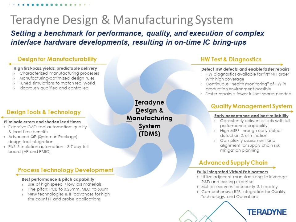
Teradyne Design & Manufacturing System (TDMS)
Teradyne understands the importance of shorter cycle times and better yields in device manufacturing— which is why DIS is focused on designing for manufacturing and reliability. We deliver a high first pass board yield so you can plan on a predictable delivery and installation schedule to support your IC bring-up and volume production ramp.
DIS uses advanced design technology to get you to your perfect design with shorter lead times. We offer advanced System in Package (SiP) design tool integration, automated full-board simulation capabilities, and extensive CAD tool automation for enhanced design and fabrication validation. Through these unique advances, combined with close co-development of manufacturing techniques and design rules with our supply chain partners, DIS ensures first pass board yields of greater than 90%.
DIS is striving continuously to enable the highest site count possible final test and wafer probe applications to maximize your tester efficiency. Currently, DIS has the capability to design and fabricate interface boards with device pin pitch down to 60µm. With DIS as your partner for device interface hardware, we’re confident your production floor will be running with the highest efficiency possible.
What about test and diagnostics for new hardware designs? Teradyne is the leader in test and that’s our specialty. On-Tester DIB-Diagnostics are possible for every new interface board, providing high fault coverage with or without a shorted-socket/wafer contact point. An extension of these diagnostic tools that integrate with the production flow provide the ability to continuously monitor the ‘health’ of a device interface board enabling early detection and diagnosis of damaged or defective components and avoidance of production test running on un-characterized hardware performance – risking poor yields or test escapes impacting downstream performance and quality.
DIS is experienced in designing, simulating, and integrating Multi-Layer Organic (MLO) space-transformer technology which enables translation of the tester signals to the fine pitch requirements of the device pins. Implementation of this unique technology enables high site count wafer probe cards with good Touch Down Efficiency (TDE).
How DIS Can Help Your Business
DIS provides you with local interface design expert resources and offers “turn-key” solutions for your interfacing needs, allowing your engineering team to focus on test development and ensuring you are able to take full advantage of the capabilities of Teradyne’s test platforms.
With over 250 global support personnel, we are a trusted partner providing local design for new device introductions. Teradyne’s experienced DIS design means our customers have a predictable hardware release schedule for mass production readiness.
If your goal is to optimize performance, quality, schedule, and total test cost for Device Interface Board (DIB) design and manufacturing, your best option is Teradyne’s Device Interface Solutions (DIS).